Zhou, Y. ; Li, J. ; Liu, L. ; Wang, C. ; Lynch, R. P. ; Bai, B. ; Hsu, H. - Y. ; Yin, Z. ; Cabot, A. ; Robinson, R. D. ; et al. Anion-Driven Enabled Functional Nanomaterials From Metal And Metal Oxide Nanoparticles.
Materials Today 2024.
AbstractDespite significant progress in the synthesis of nanocrystals (NCs) by conventional wet-chemical synthetic approaches, producing nanostructures with complex architectures tailored to specific applications remains a formidable challenge. Recently, anion-driven synthesis, including oxidation, sulfidation, phosphorization, nitridation, selenization, telluridation, and chlorination have emerged as a versatile approach to produce novel nanostructured materials with tuned size, morphology, crystal structure, and composition from the chemical transformation of template NCs. This chemical conversion can be accompanied by the formation of new NCs architectures, overall modifying the surface chemistry and the mechanical, electronic, optical, and magnetic properties of the material. This strategy can be used to optimize the performance of the material in a range of applications, including energy conversion and storage, catalysis, bioimaging, drug delivery, and sensing. In this review, we first detail the possible anion-driven synthesis and discuss the related underlying mechanisms. Subsequently, we overview the unique nanostructure obtained by this strategy and summarize their functional properties and potential applications. Finally, we provide perspectives and discuss the remaining challenges and the new opportunities in this field.
Li, Y. ; Cotlet, M. ; Hadar, I. ; Guo, P. .
Broadband Emission In Alkali Halides Triggered By Sb 3+ Doping.
Chemical Communications 2024,
60, 14806–14809.
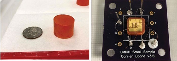
AbstractBroadband emission in a series of alkali chlorides are achieved by doping NaCl, KCl, and RbCl with Sb3+. These compounds show photoluminescence peaks in the visible range of 536–574 nm with long lifetimes in the microsecond range. Our findings could offer valuable insights for the development of new lead-free phosphors.
Zhou, Y. ; Zhang, S. ; Li, J. ; Liu, L. ; Wang, C. ; Bai, B. ; Hsu, H. - Y. ; Hadar, I. ; Yin, Z. ; Buntine, M. A. ; et al. Rational Entry-Diffusion Induced Kirkendall Effect Towards Au2S Nanotubes.
Materials Today Chemistry 2024,
38, 102029.
Abstractemiconductor nanotubes manifesting large surface area, high tensile strength, light weight, fast electron transfer kinetics and high biocompatibility have attracted tremendous attention and find widespread applications. Rational design and preparation of semiconductor nanotubes with such a unique morphology to maximum their performance and therefore, to fulfill their applications is still a challenge. Herein, we report a strategy that is capable of rationalizing entry-diffusion of Au + ions into Cu2-xS nanorods based on the Kirkendall effect, accomplishing consecutive morphology control from solid nanorods to nanotubes, and ultimately to nanorings of Au2S. The structure and composition of Au2S nanotubes were further confirmed through X-ray photoelectron spectroscopy, annular bright-field scanning transmission electron microscopy-energy dispersive spectroscopy and scanning transmission electron microscopy and Aberration-corrected transmission electron microscopy. Compared with nanorods, Au2S nanotubes demonstrated significantly enhanced catalytic activity in electrocatalytic hydrogen evolution reaction, a remarkably low overpotential of 602.0 mV at a current density of −10 mA cm−2 and a relatively low Tafel slope of 36.87 mV dec−1 in 0.5 M H2SO4 solution. It is anticipated that this novel strategy of mediating ion diffusion rate would inspire rational control of unique morphologies and structures of semiconductor nanocrystals, providing a platform for further applications based on nanomaterials
Laing, C. C. ; Kim, D. ; Park, J. ; Shen, J. ; Hadar, I. ; Hoffman, J. M. ; He, J. ; Shin, B. ; Wolverton, C. ; Kanatzidis, M. G. .
Solution-Processable Mixed-Anion Cluster Chalcohalide Rb6Re6S8I8 In A Light-Emitting Diode.
Nature materials 2024,
23, 230–236.
Abstract
Rhenium chalcohalide cluster compounds are a photoluminescent family of mixed-anion chalcohalide cluster materials. Here we report the new material RbRe₆S₈I₈, which crystallizes in the cubic space group Fm3̅m and contains isolated [Re₆S₈I₆]⁴⁻ clusters. Rb₆Re₆S₈I₈ has a band gap of 2.06(5) eV and an ionization energy of 5.51(3) eV, and exhibits broad photoluminescence (PL) ranging from 1.01 eV to 2.12 eV. The room-temperature PL exhibits a PL quantum yield of 42.7% and a PL lifetime of 77 μs (99 μs at 77 K). Rb₆Re₆S₈I₈ is found to be soluble in multiple polar solvents including N,N-dimethylformamide, which enables solution processing of the material into films with thickness under 150 nm. Light-emitting diodes based on films of Rb₆Re₆S₈I₈ were fabricated, demonstrating the potential for this family of materials in optoelectronic devices.