Cai, S. ; Hao, S. ; Luo, Z. - Z. ; Li, X. ; Hadar, I. ; Bailey, T. ; Hu, X. ; Uher, C. ; Hu, Y. - Y. ; Wolverton, C. ; et al. Discordant Nature Of Cd In Pbse: Off-Centering And Core-Shell Nanoscale Cdse Precipitates Lead To High Thermoelectric Performance.
ENERGY & ENVIRONMENTAL SCIENCE 2020,
13, 200-211.
Publisher's VersionAbstractWe report a novel hierarchical microstructure in the PbSe–CdSe system, which collectively contributes to significant enhancement in thermoelectric performance, with ZTave ∼ 0.83 across the 400–923 K temperature range, the highest reported for p-type, Te-free PbSe systems. We have investigated the local atomic structure as well as the microstructure of a series of PbSe–xCdSe materials, up to x = 10%. We find that the behavior of the Cd atoms in the octahedral rock salt sites is discordant and results in off-center displacement and distortion. Such off-centered Cd in the PbSe matrix creates (1) L–Σ electronic energy band convergence, (2) a flattened L band, both contributing to higher Seebeck coefficients, and (3) enhanced phonon scattering, which leads to lower thermal conductivity. These conclusions are supported by photoemission yield spectroscopy in air (PYSA), solid state 111Cd, 77Se NMR spectroscopy and DFT calculations. Above the solubility limit (>6%CdSe), we also observe endotaxial CdSe nano-precipitates with core–shell architecture formed in PbSe, whose size, distribution and structure gradually change with the Cd content. The nano-precipitates exhibit a zinc blende crystal structure and a tetrahedral shape with significant local strain, but are covered with a thin wurtzite layer along the precipitate/matrix interface, creating a core–shell structure embedded in PbSe. This newly discovered architecture causes a further reduction in lattice thermal conductivity. Moreover, potassium is found to be an effective p-type dopant in the PbSe–CdSe system, leading to an enhanced power factor, a maximum ZT of ∼1.4 at 923 K for Pb0.98K0.02Se–6%CdSe.

Luo, Y. ; Cai, S. ; Hao, S. ; Pielnhofer, F. ; Hadar, I. ; Luo, Z. - Z. ; Xu, J. ; Wolverton, C. ; Dravid, V. P. ; Pfitzner, A. ; et al. High-Performance Thermoelectrics From Cellular Nanostructured Sb2Si2Te6.
JOULE 2020,
4, 159-175.
Publisher's VersionAbstractWe introduce Sb2Si2Te6 as a high-performance thermoelectric material. Single-crystal X-ray diffraction analysis indicates that Sb2Si2Te6 has a layered two-dimensional structure with Sb3+ cations and [Si2Te6]6− units as building blocks adopting the Fe2P2Se6 structure type. Sb2Si2Te6 is a direct-band-gap semiconductor with valence-band maximum and conduction-band minimum at the Z point in the Brillouin zone, where the band is doubly degenerate. Polycrystalline bulk pellets of Sb2Si2Te6 with randomly packed grains exhibit an intrinsically high thermoelectric figure of merit ZT of ∼1.08 at 823 K. We then create a cellular nanostructure with ultrathin Si2Te3 nanosheets covering the Sb2Si2Te6 grains, which act as a hole-transmitting electron-blocking filter and at the same time cause extra phonon scattering. This dual function of the cellular nanostructure achieves an ultralow thermal conductivity value of ∼0.29 Wm−1K−1 and a high ZT value of ∼1.65 at 823 K for Sb2Si2Te6, along with a high average ZT value of ∼0.98.

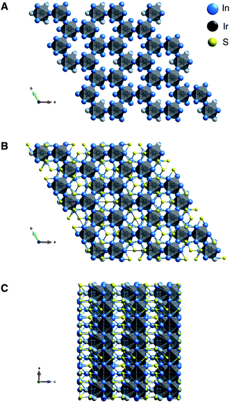
Khoury, J. F. ; He, J. ; Pfluger, J. E. ; Hadar, I. ; Balasubramanian, M. ; Stoumpos, C. C. ; Zu, R. ; Gopalan, V. ; Wolverton, C. ; Kanatzidis, M. G. .
Ir6In32S21, A Polar, Metal-Rich Semiconducting Subchalcogenide.
CHEMICAL SCIENCE 2020,
11, 870-878.
Publisher's VersionAbstractSubchalcogenides are uncommon, and their chemical bonding results from an interplay between metal–metal and metal–chalcogenide interactions. Herein, we present Ir6In32S21, a novel semiconducting subchalcogenide compound that crystallizes in a new structure type in the polar P31m space group, with unit cell parameters a = 13.9378(12) Å, c = 8.2316(8) Å, α = β = 90°, γ = 120°. The compound has a large band gap of 1.48(2) eV, and photoemission and Kelvin probe measurements corroborate this semiconducting behavior with a valence band maximum (VBM) of −4.95(5) eV, conduction band minimum of −3.47(5) eV, and a photoresponse shift of the Fermi level by ∼0.2 eV in the presence of white light. X-ray absorption spectroscopy shows absorption edges for In and Ir do not indicate clear oxidation states, suggesting that the numerous coordination environments of Ir6In32S21 make such assignments ambiguous. Electronic structure calculations confirm the semiconducting character with a nearly direct band gap, and electron localization function (ELF) analysis suggests that the origin of the gap is the result of electron transfer from the In atoms to the S 3p and Ir 5d orbitals. DFT calculations indicate that the average hole effective masses near the VBM (1.19me) are substantially smaller than the average electron masses near the CBM (2.51me), an unusual feature for most semiconductors. The crystal and electronic structure of Ir6In32S21, along with spectroscopic data, suggest that it is neither a true intermetallic nor a classical semiconductor, but somewhere in between those two extremes.
Li, X. ; Fu, Y. ; Pedesseau, L. ; Guo, P. ; Cuthriell, S. ; Hadar, I. ; Even, J. ; Katan, C. ; Stoumpos, C. C. ; Schaller, R. D. ; et al. Negative Pressure Engineering With Large Cage Cations In 2D Halide Perovskites Causes Lattice Softening.
JOURNAL OF THE AMERICAN CHEMICAL SOCIETY 2020,
142, 11486-11496.
Publisher's VersionAbstractOrganic–inorganic hybrid halide perovskites are promising semiconductors with tailorable optical and electronic properties. The choice of A-site cation to support a three-dimensional (3D) perovskite structure AMX3 (where M is a metal and X is a halide) is limited by the geometric Goldschmidt tolerance factor. However, this geometric constraint can be relaxed in two-dimensional (2D) perovskites, providing us an opportunity to understand how various A-site cations modulate the structural properties and thereby the optoelectronic properties. Here, we report the synthesis and structures of single-crystal (BA)2(A)Pb2I7 where BA = butylammonium and A = methylammonium (MA), formamidinium (FA), dimethylammonium (DMA), or guanidinium (GA), with a series of A-site cations varying in size. Single-crystal X-ray diffraction reveals that the MA, FA, and GA structures crystallize in the same Cmcm space group, while the DMA imposes the Ccmb space group. We observe that as the A-site cation becomes larger, the Pb–I bond continuously elongates, expanding the volume of the perovskite cage, equivalent to exerting “negative pressure” on the perovskite structures. Optical studies and DFT calculations show that the Pb–I bond length elongation reduces the overlap of the Pb s- and I p-orbitals and increases the optical bandgap, while Pb–I–Pb tilting angles play a secondary role. Raman spectra show lattice softening with increasing size of the A-site cation. These structural changes with enlarged A cations result in significant decreases in photoluminescence intensity and lifetime, consistent with a more pronounced nonradiative decay. Transient absorption microscopy results suggest that the PL drop may derive from a higher concentration of traps or phonon-assisted nonradiative recombination. The results highlight that extending the range of Goldschmidt tolerance factors for 2D perovskites is achievable, enabling further tuning of the structure–property relationships in 2D perovskites.

Hoffman, J. M. ; Malliakas, C. D. ; Sidhik, S. ; Hadar, I. ; McClain, R. ; Mohite, A. D. ; Kanatzidis, M. G. .
Long Periodic Ripple In A 2D Hybrid Halide Perovskite Structure Using Branched Organic Spacers.
CHEMICAL SCIENCE 2020,
11, 12139-12148.
Publisher's VersionAbstractTwo-dimensional (2D) halide perovskites have great promise in optoelectronic devices because of their stability and optical tunability, but the subtle effects on the inorganic layer when modifying the organic spacer remain unclear. Here, we introduce two homologous series of Ruddlesden-Popper (RP) structures using the branched isobutylammonium (IBA) and isoamylammonium (IAA) cations with the general formula (RA)(2)(MA)(n-1)PbnI3n+1 (RA = IBA, IAA; MA = methylammonium n = 1-4). Surprisingly, the IAA n = 2 member results in the first modulated 2D perovskite structure with a ripple with a periodicity of 50.6 angstrom occurring in the inorganic slab diagonally to the [101] direction of the basic unit cell. This leads to an increase of Pb-I-Pb angles along the direction of the wave. Generally, both series show larger in-plane bond angles resulting from the additional bulkiness of the spacers compensating for the MA's small size. Larger bond angles have been shown to decrease the bandgap which is seen here with the bulkier IBA leading to both larger in-plane angles and lower bandgaps except for n = 2, in which the modulated structure has a lower bandgap because of its larger Pb-I-Pb angles. Photo-response was tested for the n = 4 compounds and confirmed, signaling their potential use in solar cell devices. We made films using an MACl additive which showed good crystallinity and preferred orientation according to grazing-incidence wide-angle scattering (GIWAXS). As exemplar, the two n = 4 samples were employed in devices with champion efficiencies of 8.22% and 7.32% for IBA and IAA, respectively.
Ke, W. ; Chen, C. ; Spanopoulos, I. ; Mao, L. ; Hadar, I. ; Li, X. ; Hoffman, J. M. ; Song, Z. ; Yan, Y. ; Kanatzidis, M. G. .
Narrow-Bandgap Mixed Lead/Tin-Based 2D Dion-Jacobson Perovskites Boost The Performance Of Solar Cells.
JOURNAL OF THE AMERICAN CHEMICAL SOCIETY 2020,
142, 15049-15057.
Publisher's VersionAbstractThe advent of the two-dimensional (2D) family of halide perovskites and their demonstration in 2D/three-dimensional (3D) hierarchical film structures broke new ground toward high device performance and good stability. The 2D Dion–Jacobson (DJ) phase halide perovskites are especially attractive in solar cells because of their superior charge transport properties. Here, we report on 2D DJ phase perovskites using a 3-(aminomethyl)piperidinium (3AMP) organic spacer for the fabrication of mixed Pb/Sn-based perovskites, exhibiting a narrow bandgap of 1.27 eV and a long carrier lifetime of 657.7 ns. Consequently, solar cells employing mixed 2D DJ 3AMP-based and 3D MA0.5FA0.5Pb0.5Sn0.5I3 (MA = methylammonium, FA = formamidinium) perovskite composites as light absorbers achieve enhanced efficiency and stability, giving a power conversion efficiency of 20.09% with a high open-circuit voltage of 0.88 V, a fill factor of 79.74%, and a short-circuit current density of 28.63 mA cm–2. The results provide an effective strategy to improve the performance of single-junction narrow-bandgap solar cells and, potentially, to give a highly efficient alternative to bottom solar cells in tandem devices.


